Projects Brainstorming
TIP
What you are about to read down here is probably gibberish
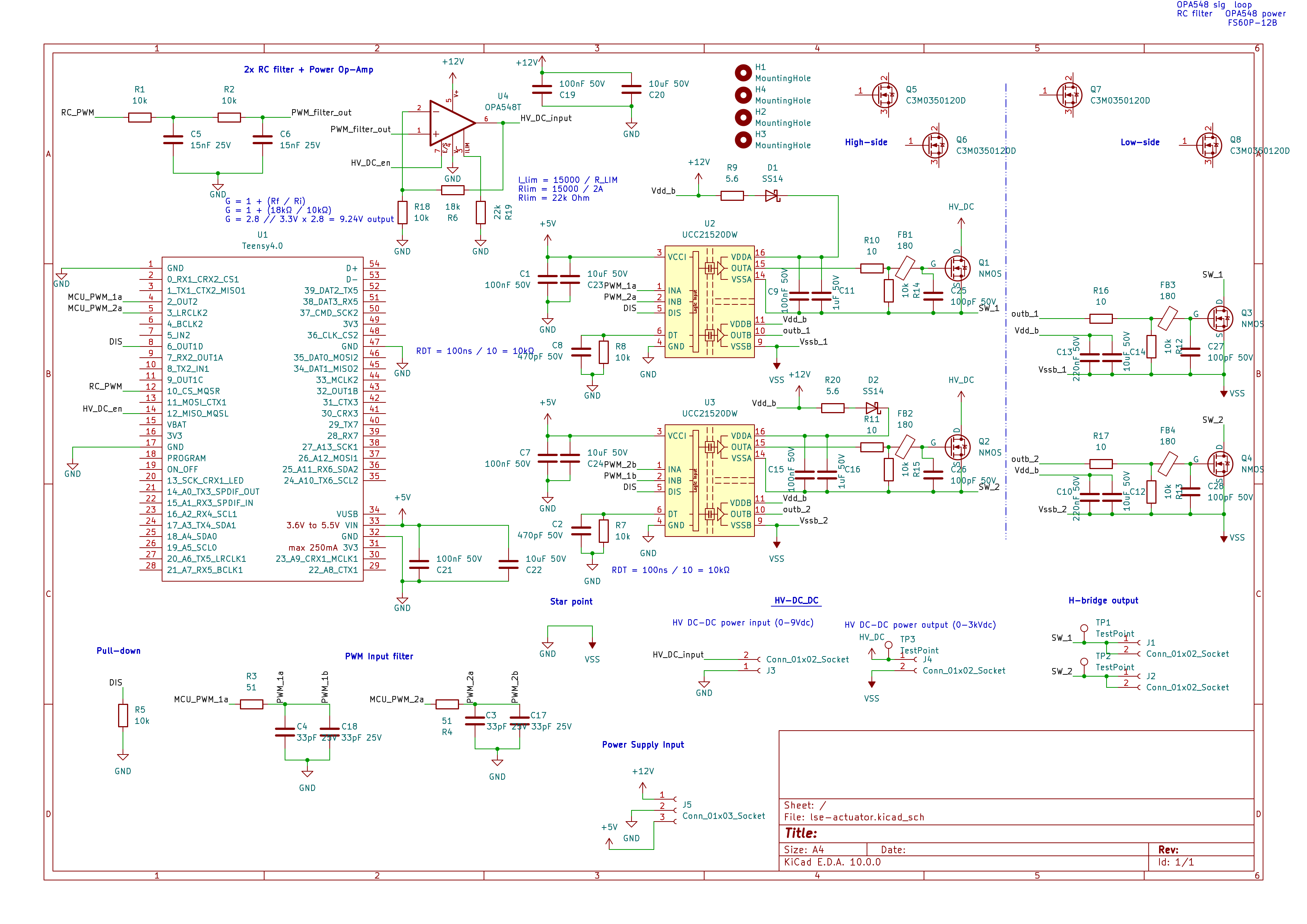
Liquid Crystal Elastomer (LCE) Actuator with H-Bridge
Updated - 03/03/2026
- INA/INB TTL high threshold is 1.8V, can be use with wide range of MCU voltage level from as low as 3.3V. That said, the amplitude of any signal applied to INA or INB must never be at a voltage higher than VCCI.
- DT (Disable Time) pin can be program by placing Rdt to ground: Tdt = 10 x Rdt. pair with a capacitor =<1nF. Not recommended to leave it floating. RDT = 100ns / 10 = 10kΩ
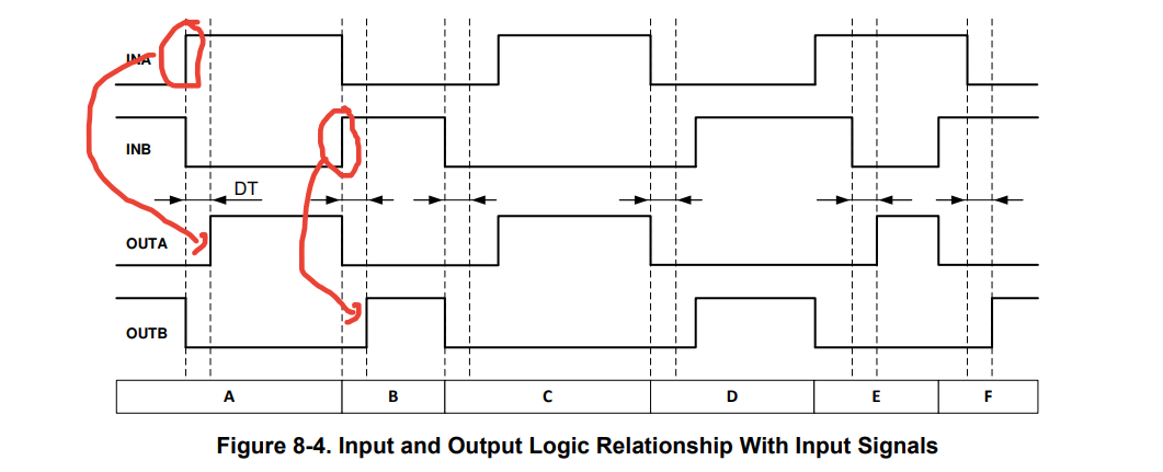
Condition A: INB goes low, INA goes high. INB sets OUTB low immediately and assigns the programmed dead time to OUTA. OUTA is allowed to go high after the programmed dead time.
Condition B: INB goes high, INA goes low. Now INA sets OUTA low immediately and assigns the programmed dead time to OUTB. OUTB is allowed to go high after the programmed dead time.
Condition C: INB goes low, INA is still low. INB sets OUTB low immediately and assigns the programmed dead time for OUTA. In this case, the input signal’s own dead time is longer than the programmed dead time. Thus, when INA goes high, it immediately sets OUTA high
Condition D: INA goes low, INB is still low. INA sets OUTA low immediately and assigns the programmed dead time to OUTB. INB’s own dead time is longer than the programmed dead time. Thus, when INB goes high, it immediately sets OUTB high.
Condition E: INA goes high, while INB and OUTB are still high. To avoid overshoot, INA immediately pulls OUTB low and keeps OUTA low. After some time OUTB goes low and assigns the programmed dead time to OUTA. OUTB is already low. After the programmed dead time, OUTA is allowed to go high.
Condition F: INB goes high, while INA and OUTA are still high. To avoid overshoot, INB immediately pulls OUTA low and keeps OUTB low. After some time OUTA goes low and assigns the programmed dead time to OUTB. OUTA is already low. After the programmed dead time, OUTB is allowed to go high.
Typical application
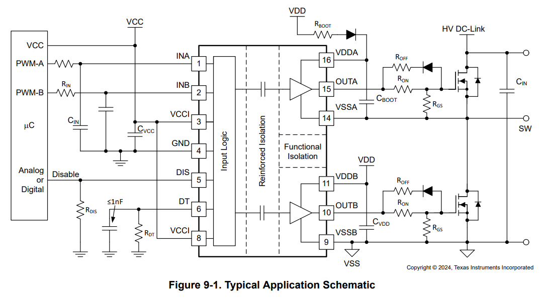
Selecting Rboot and Diode (Vdd - Vbdf) / rboot = A, amount of current limit rushing through. Vdd = input power supply Vbdf = Diode forward voltage, Vf
Using SS14 Schottky diode, with Vf of 0.5V (12V - 0.5V) / 2A = 5.75 Ohm, the closes in E24 series is 5.6 Ohm, which resulted in the maximum in-rush current of 2.05A
Circuit Diagram
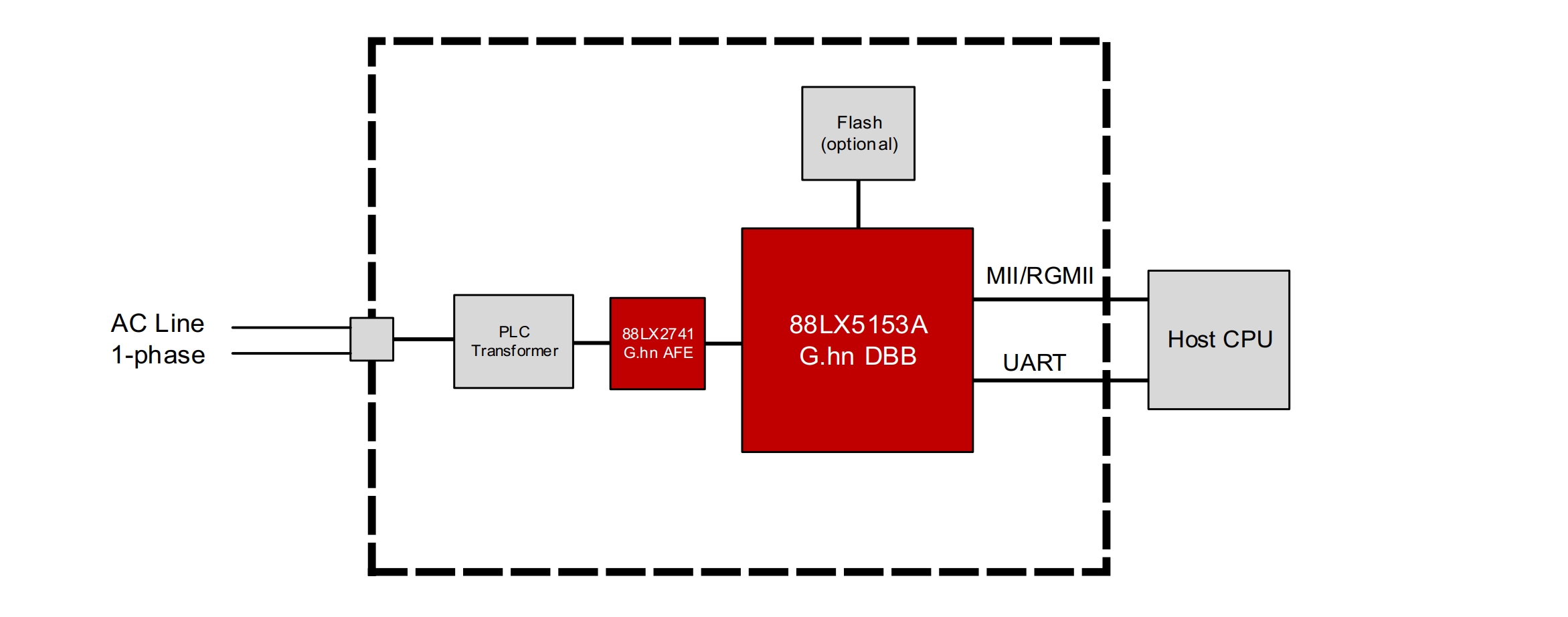
Powerline (PLC) KVM switch FPGA
Updated - 29/01/2026
First project to get my foot into FPGAs world, this will probably take 3 years to achieve. But we are here for the long haul don’t we? Aite here we go.
FPGA: Xilinx Artix-7, XC7A35T-1FTG256C
PLC IC/Modem: MaxLinear 88LX5152 Wave-2 G.hn standard Digital Baseband (DBB) Processor
Analog Front End (AFE): MaxLinear 88LX2720 G.hn Wave-2 Analog Front End (AFE) for Powerline
Target bit rate: no idea really, raw HDMI output is at Gb. Need to find way to compressed it.
This project going to leave me financially cripple. That’s all I got… To Be Continue on Dragon Ball Z…
Komputer Basikal, KB-01 (Bike Computer)
Updated - 05/02/2026
| Specification | Description |
|---|---|
| SBC | Raspberry Pi CM5 4GB |
| Storage | NVMe 250GB M.2 2230 |
| GNSS | ST Teseo-LIV4F |
| Antenna | Taoglas FXP611.07.0092C (passive antenna) |
| Display | Waveshare 3.5inch DSI LCD H/E |
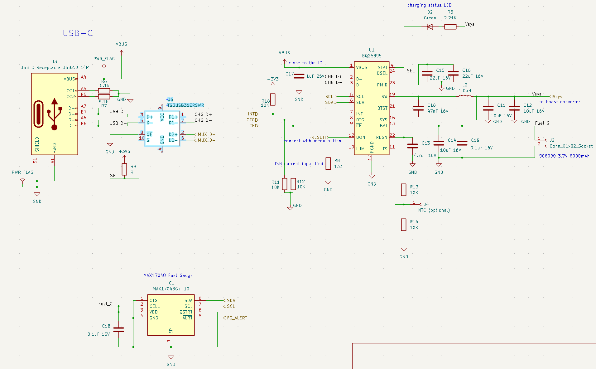
| Battery | 10,000mAh Li-ion (1160100) |
| BMS | TI BQ25895 |
| Fuel Gauge | Maxim MAX17048 |
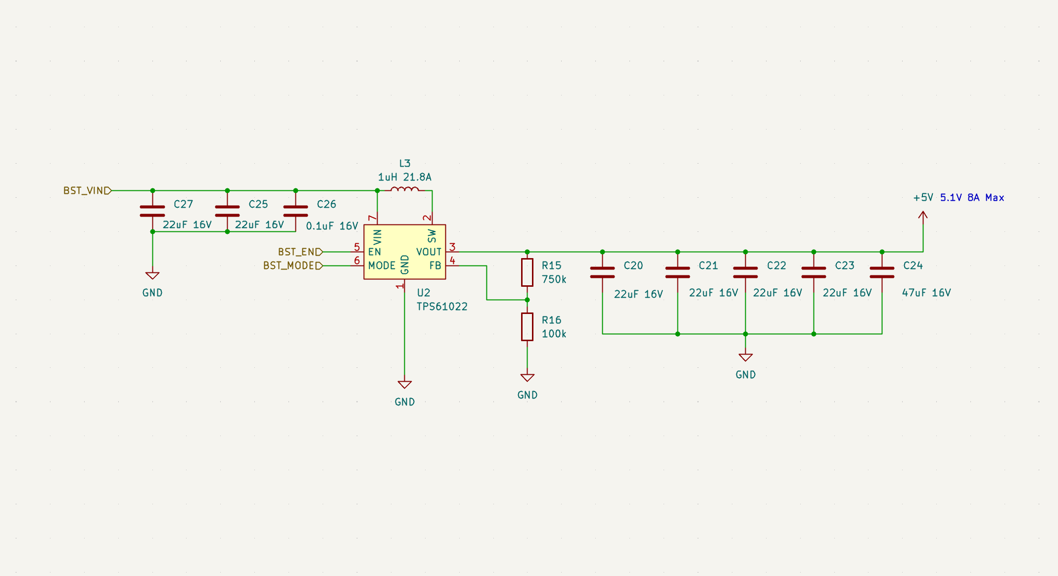
| PSU Boost IC | TI TPS61022 |
| USB Mux | TI TS3USB30E |
| Audio | Passive buzzer (CMT-0502-03-SMT-TR) |
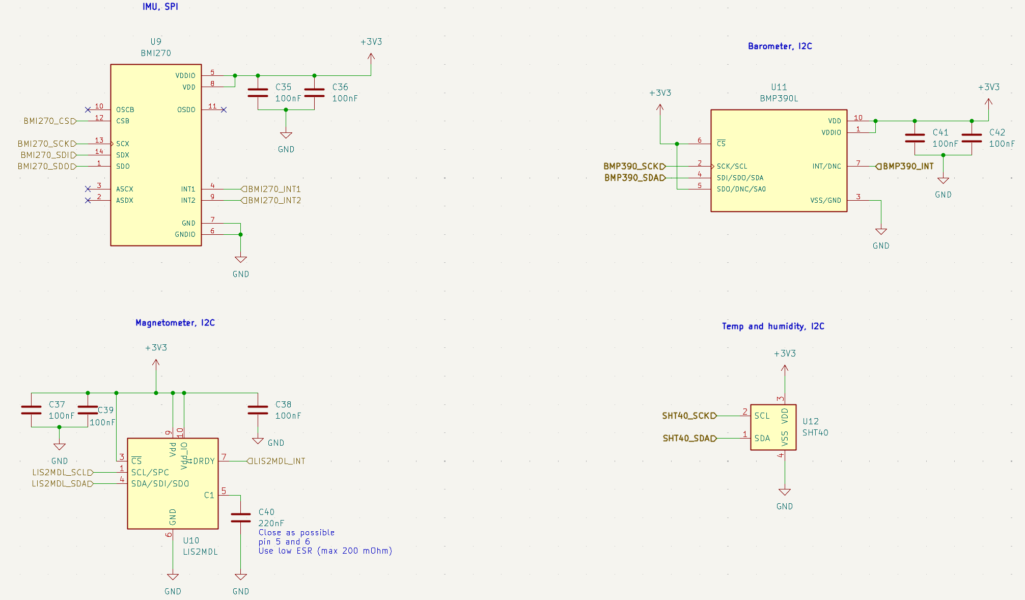
Sensor
| Sensor | Description |
|---|---|
| IMU | Bosch BMI270 |
| Magnetometer | ST LIS2MDL |
| Barometer | Bosch BMP390 |
| Temp/Humidity | Sensirion SHT40 |
| Wheel Speed | TI DRV5023AJ |
Circuit Block
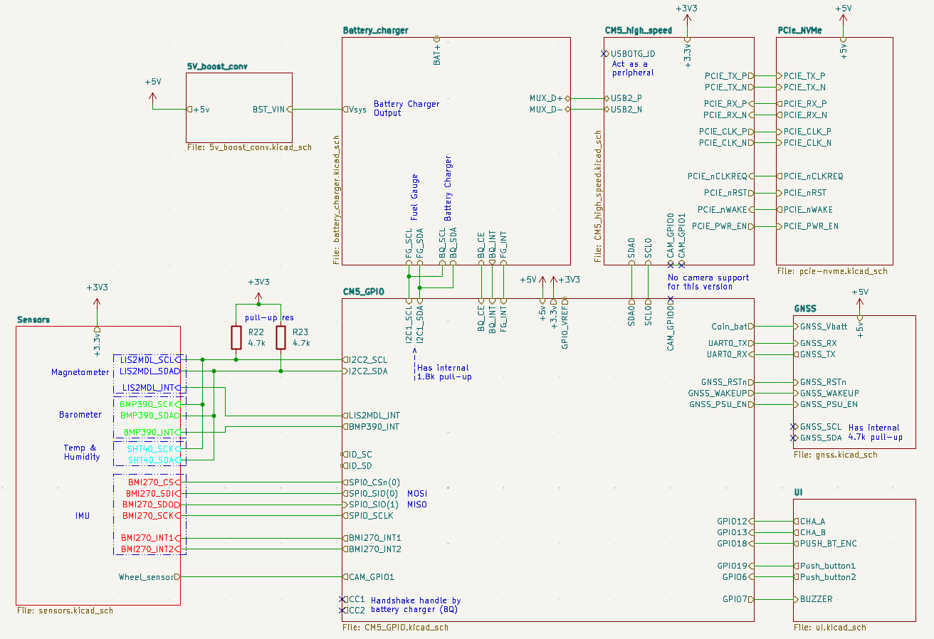
There’s 4 different sensor, only one is interfacing with SPI (IMU) while the other is with I2C. For machine learning dead reckoning, I will need to get a lot of IMU data, since SPI is faster than I2C, it sort of make sense. The rest is not so critical. Need load of data to train a model. I am planning to add another one that is a wheel speed sensor but this is an external sensor (away from PCB), need to figure out how…
Battery Management System IC: TI BQ25895
A charger pass-through battery charging IC, can charge and directing the power to the SBC simultaneously. Adding an USB 2.0 multiplexer can connect to a host device (i.e. laptop) transfer data while charging, smart innit?
PSU Boost IC: TI TPS61022
A constant boost IC that supply fixed voltage at 5.1V with 8A maximum which give enough head room to power the SBC at 4A and the NVMe drive. With 1.5MHz switching frequency means small footprint, will it create EMC problem down the line? Nobody knows ¯\_(ツ)_/¯ we’ll find out soon how bad is my routing.
Main storage: 250GB NVMe 2230
Purely based on the CM5 IO carrier board. Opt for a higher clearance M.2 slot so that I can place the step down converter under NVMe drive, save some space. Note to self; make sure the drive is only populated on one side.
For a bike-computer, this prolly don’t make sense at all. Literally designing a PDA device. Bet it wont last even an hour of operation. Heh, at least we learn by doing mistake don’t we (。_。) [flashing through me eyes all the failed projects]
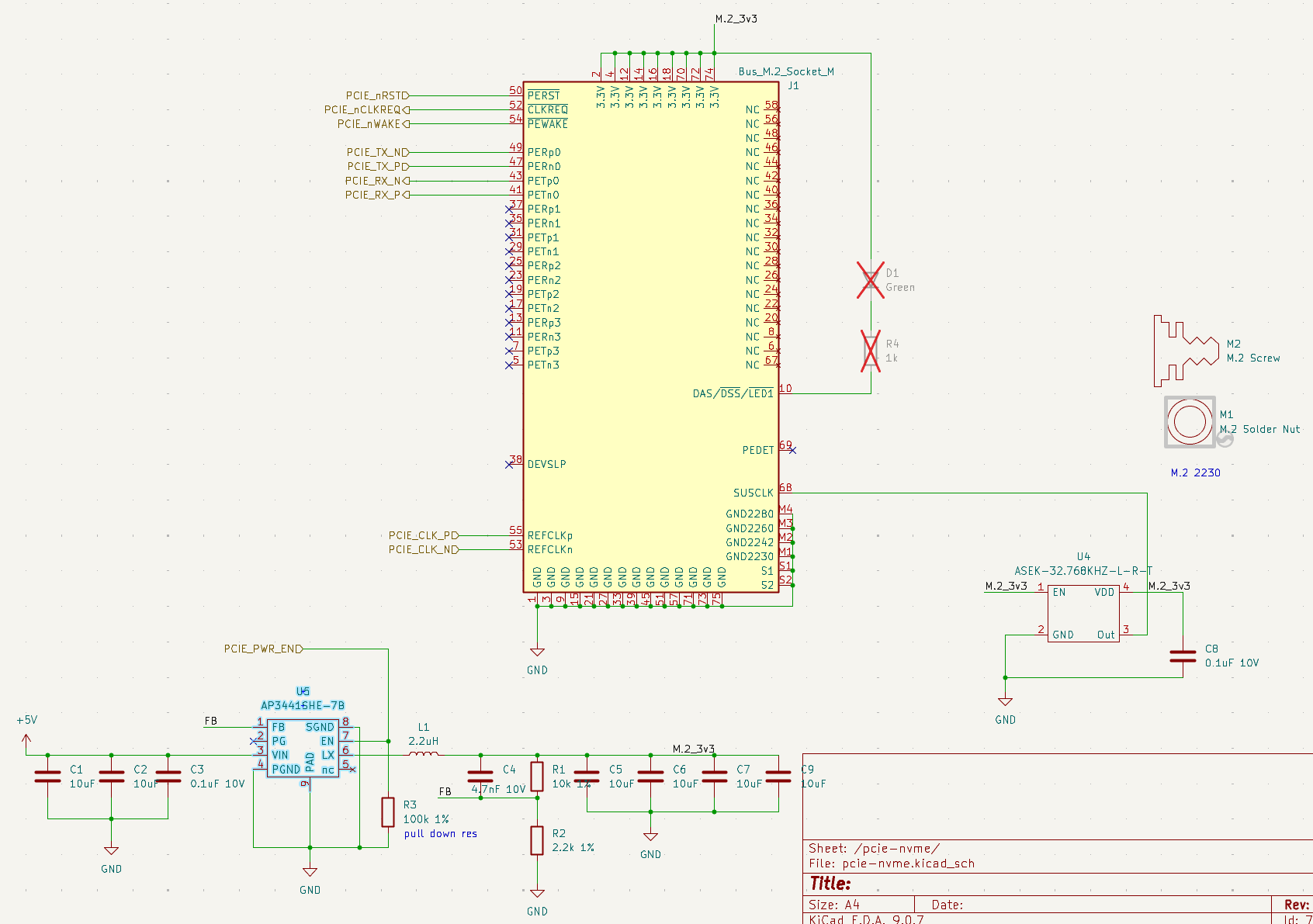
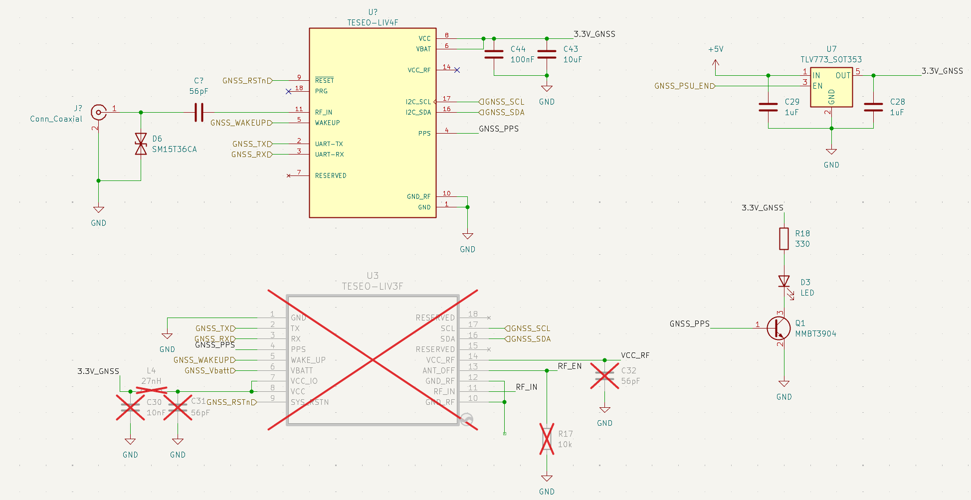
GNSS Module: ST Teseo-LIV4F LIV3F
It’s small and affordable GNSS module. At first I was planning to use an all-in-one module (built-in antenna). Problem is, the signal might be horrible due to casing. External passive antenna like Taoglas FXP611.07.0092C, can be move to face the sky directly and since it is passive, does not consume much battery. Circuitry mainly based on Digikey own GNSS module breakout design and LIV3F hardware manual. Hope the PCB design track is not much of a hassle to design.
Update: 11/02/26

Decided to yeet out LIV3F for LIV4F, same footprint but with multichannel (L1 and L5) GNSS, this will give more accurate reading (under 1m accuracy). And I don’t need to worry about the front-end analog, built-in LNA and SAW filter.
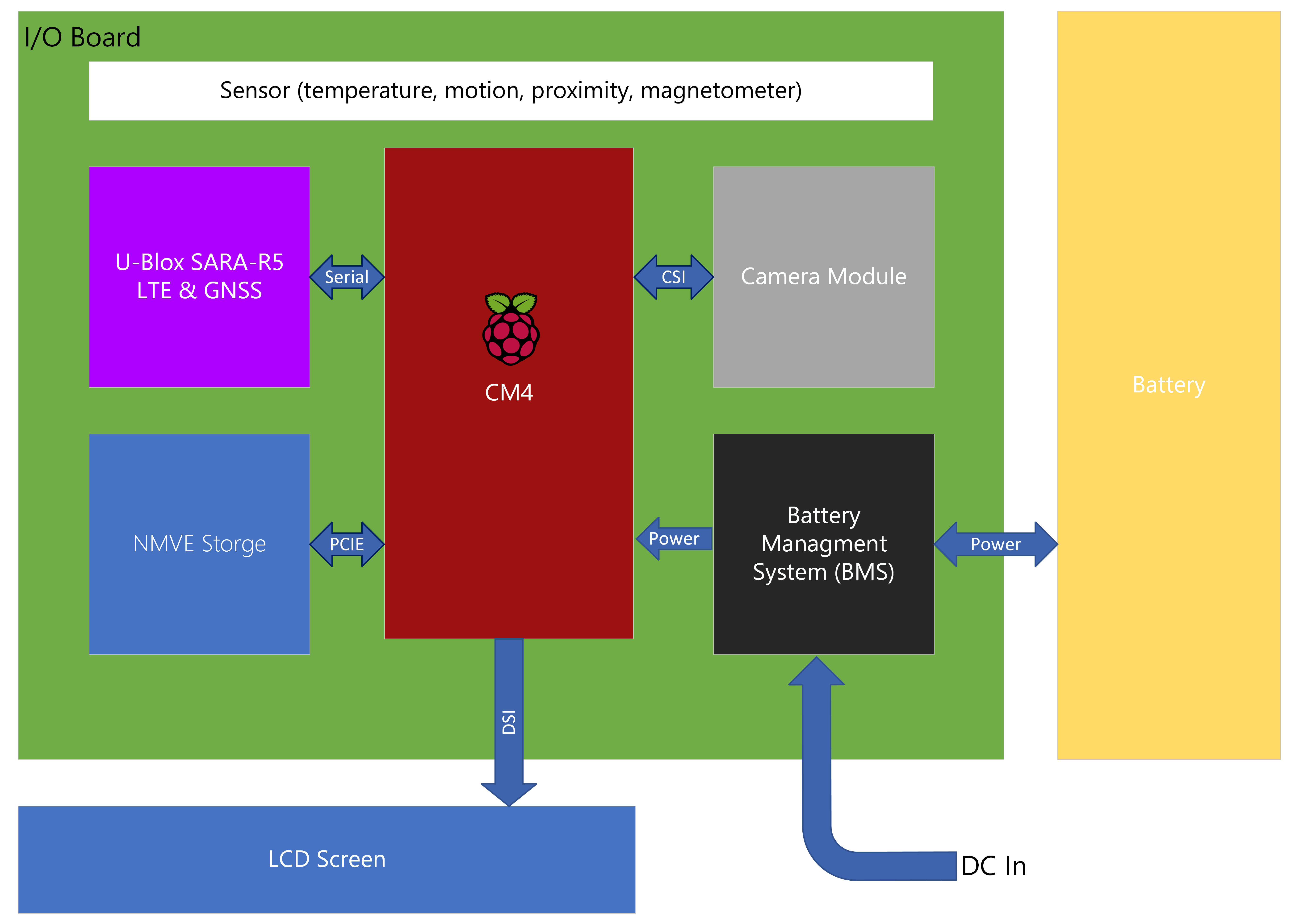
RVDR+
Commencing July 2023
This is my fourth PCB project in the making. Just a bunch of ideas that I could think of.
Component to consider:
- CM4 as main CPU
- Utilize PCIe for storage
- U-blox SARA-R5 series for LTE and GNSS connectivity (SIM card or E-SIM?)
- powered with battery, need utilized low-power design (power supply design)
- Camera module for recording purposes
- Various sensors; temperature, motion, proximity, magnetometer
- Display with touch screen capability? (needed further research)
Software:
- Plate recognition (OpenCV and in C++)
- MQTT client
link kept as reference for Electronic Design:
- BMS/Power supply Design for CM4
- PiJuice
- PowerBoost 1000 Charger
- CM4-POE-UPS-BASE
- BQ24160 ACTIVE I2C 1cell 2.5A Buck battery charger with dual-input, Power Path and USB detection
- Raspberry Pi PCIe Devices
- Lecture notes: Battery Management and Control
- SparkFun MicroMod Asset Tracker Carrier Board, Ublox SARA-R5
- RPi CM4 - LiM Carrier Board series
Breakout board
More info to be added soon
Tuah-one resources
Link for project build reference:
- Flashing the Atmega32A
- Mechanical Keyboard Prototype With V-USB & QMK
- How to burn the Plaid keyboard bootloader using Arduino Nano
The command for the avrdude:
avrdude -c stk500v1 -P COM12 -p m32a -U flash:w:C:/Users/ucems09/qmk_firmware/coseyfannitutti_discipline_default.hex:i -v -b 19200
-c stk500v1use stk500 version 1 as the programmer.-P COM12port value, for this it is COM12, can check Arduino IDE.-p m32atype of MCU, for this it is m32a for Atmega32A.-u flash:w:C:/Users/ucems09/qmk_firmware/coseyfannitutti_discipline_default.hex:iprogram to be flashed in hex format.-vjust more information in the CLI.-b 19200set the baudrate this is 19200, was burn by the arduino ISP, very important to set the baudrate.